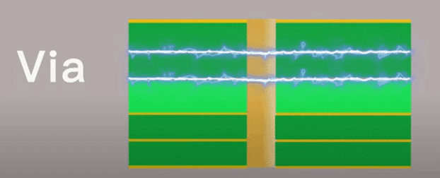
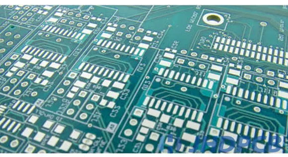
PCBWay Via Plating Thickness: The Key to Quality PCB Manufacturing! via-in-pad in pcb design manufacturing
If you are searching about The Ultimate Guide to Understanding Via Plating Thickness in PCBs - Top you've came to the right web. We have 25 Images about The Ultimate Guide to Understanding Via Plating Thickness in PCBs - Top like Detailed Procedures of Plating Copper for PCB Processing - PCB, Detailed Procedures of Plating Copper for PCB Processing - PCB and also Detailed Procedures of Plating Copper for PCB Processing - PCB. Read more:
The Ultimate Guide To Understanding Via Plating Thickness In PCBs - Top
 camtechpcb.com
The Ultimate Guide to Understanding Via Plating Thickness in PCBs - Top ...
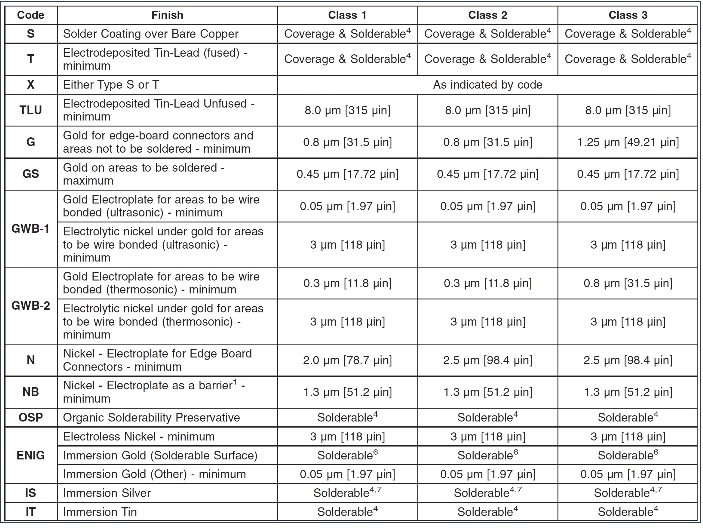
IPC Standards For Surface Plating
 www.sharedpcb.com
IPC Standards for Surface Plating
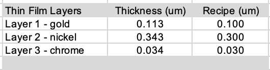
Plating Thickness Measurements - SEM Lab Inc.
 www.semlab.com
Plating Thickness Measurements - SEM Lab Inc.
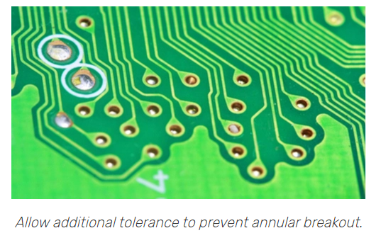
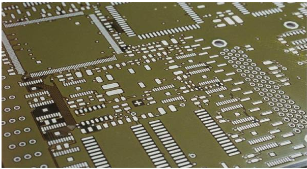
Detailed Procedures Of Plating Copper For PCB Processing - PCB
 www.pcbway.com
Detailed Procedures of Plating Copper for PCB Processing - PCB ...
The Ultimate Guide To Understanding Via Plating Thickness In PCBs - Top
 camtechpcb.com
The Ultimate Guide to Understanding Via Plating Thickness in PCBs - Top ...
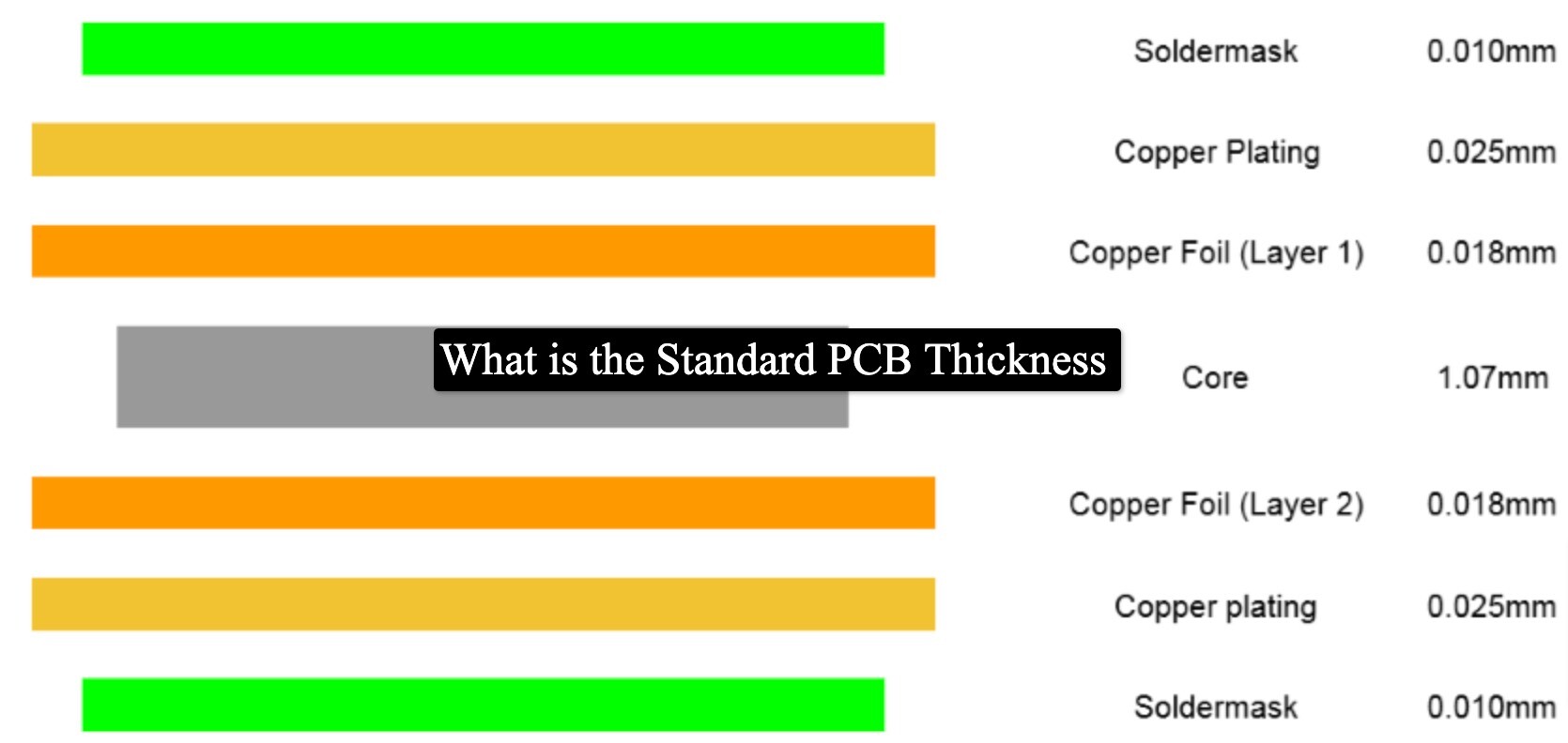
Standard PCB Thickness - Everything You Need To Know About
 absolutepcbassembly.com
Standard PCB Thickness - Everything you need to know about
The Ultimate Guide To Understanding Via Plating Thickness In PCBs - Top
 camtechpcb.com
The Ultimate Guide to Understanding Via Plating Thickness in PCBs - Top ...
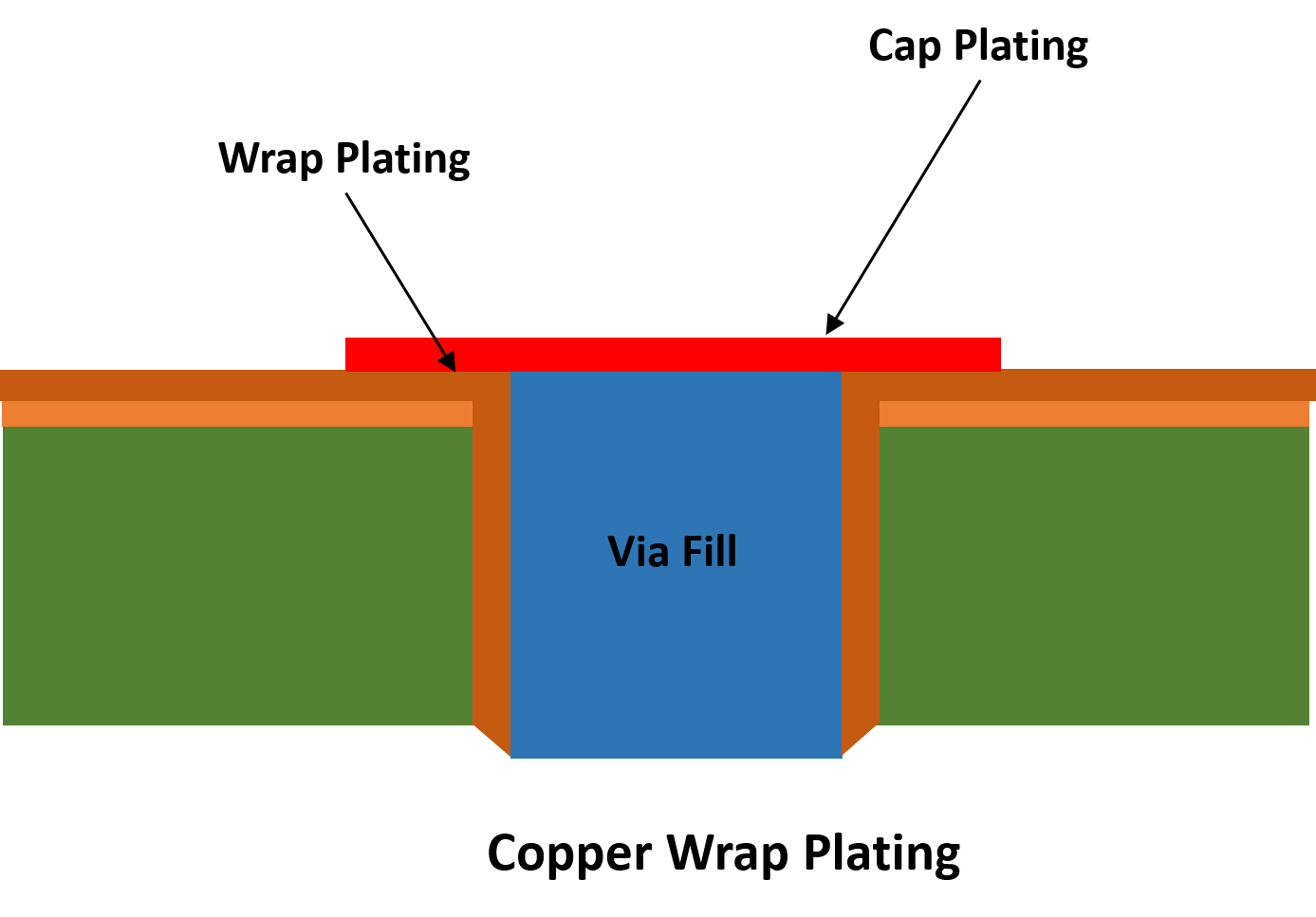
Copper Wrap Plating For PCB Manufacturing | Sierra Circuits
 www.protoexpress.com
Copper Wrap Plating for PCB Manufacturing | Sierra Circuits
Explaining Via-filling Plating In PCB Manufacturing Process - RayPCB
 www.raypcb.com
Explaining Via-filling Plating in PCB Manufacturing Process - RayPCB
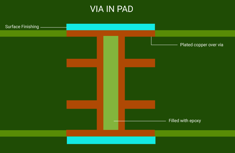
Via-in-Pad In PCB Design Manufacturing | Sierra Circuits
 www.protoexpress.com
Via-in-Pad in PCB Design Manufacturing | Sierra Circuits
Inspirasi Pcbway Via Plating Thickness, Skema Pcb
 skemadriver.blogspot.com
Inspirasi Pcbway Via Plating Thickness, Skema Pcb
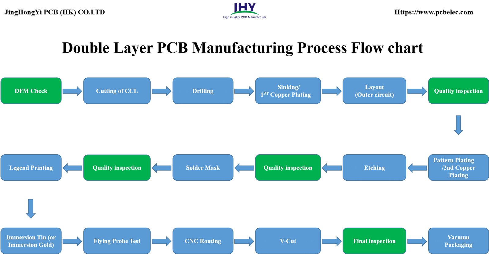
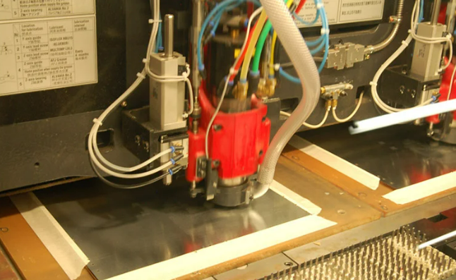
Double-sided PCB Manufacturing Process Flowchart And Step By Step
 www.pcbelec.com
Double-sided PCB Manufacturing Process Flowchart and Step by Step
The Ultimate Guide To Understanding Via Plating Thickness In PCBs - Top
 camtechpcb.com
The Ultimate Guide to Understanding Via Plating Thickness in PCBs - Top ...
The Ultimate Guide To Understanding Via Plating Thickness In PCBs - Top
 camtechpcb.com
The Ultimate Guide to Understanding Via Plating Thickness in PCBs - Top ...
Standard PCB Thickness - Determine The Right Standards
 www.ourpcb.com
Standard PCB Thickness - Determine the Right Standards
Inspirasi Pcbway Via Plating Thickness, Skema Pcb
 skemadriver.blogspot.com
Inspirasi Pcbway Via Plating Thickness, Skema Pcb
PCB Via Plating: Depth Guide And Process - Jhdpcb
 jhdpcb.com
PCB Via Plating: Depth Guide And Process - Jhdpcb
Why Some PCBs Need Edge Plating? - Technology - PCBway
 www.pcbway.com
Why Some PCBs Need Edge Plating? - Technology - PCBway
Detailed Procedures Of Plating Copper For PCB Processing - PCB
 www.pcbway.com
Detailed Procedures of Plating Copper for PCB Processing - PCB ...
Inspirasi Pcbway Via Plating Thickness Skema Pcb - Vrogue.co
 www.vrogue.co
Inspirasi Pcbway Via Plating Thickness Skema Pcb - vrogue.co
The Ultimate Guide To Understanding Via Plating Thickness In PCBs - Top
 camtechpcb.com
The Ultimate Guide to Understanding Via Plating Thickness in PCBs - Top ...
Selective Gold Plating PCB - FX PCB
 sfxpcb.com
Selective Gold Plating PCB - FX PCB
The Ultimate Guide To Understanding Via Plating Thickness In PCBs - Top
 camtechpcb.com
The Ultimate Guide to Understanding Via Plating Thickness in PCBs - Top ...
Inspirasi Pcbway Via Plating Thickness, Skema Pcb
 skemadriver.blogspot.com
Inspirasi Pcbway Via Plating Thickness, Skema Pcb
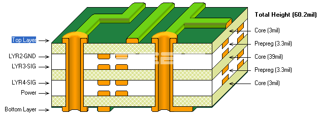
Pcb Design - PCB Base Copper Weight Vs Plating Thickness - Electrical
 electronics.stackexchange.com
pcb design - PCB base copper weight vs plating thickness - Electrical ...
Inspirasi pcbway via plating thickness, skema pcb. Inspirasi pcbway via plating thickness, skema pcb. The ultimate guide to understanding via plating thickness in pcbs